State Of The Art Single Layer or Double Layer DIY PCB Production
with FR4 or aluminum substrate
After many years of DIY electronic projects, I can share my experience about having state of the art electronic PCBs, time after time, with zero or at least minimal initial errors.
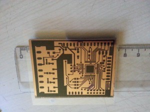
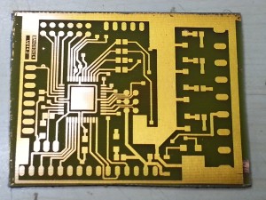
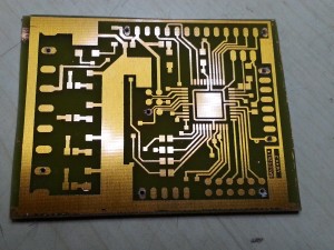
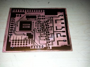
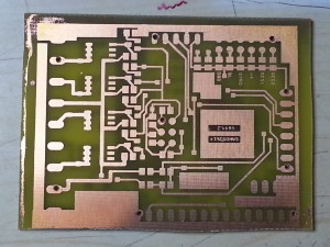
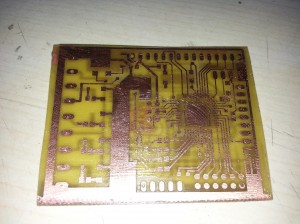
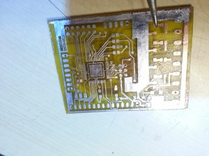
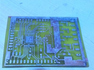
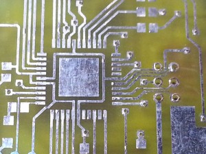
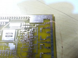
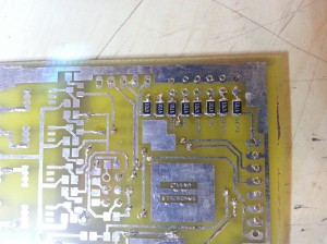
I have chosen a double sided PCB as example, with a size of 50×37 mm (1.97×1.46 inches). This will show what to expect if following the instructions below.
If you like my tutorial, you know what to do.
The many things incurred in the process will be explained thoroughly and I wish you all the best results, similar to mine.
1. NECESSARY MATERIALS
a. presensitive PCBs or Positive-sprayed PCBs;
Presensitive PCBs are commercially available PCBs covered with a thin layer of photo-sensitive laquer, protected by a plastic layer which doesn’t allow for light to gain the photosensitive layer until the time of etching. These PCBs come in simple or double copper layered models.
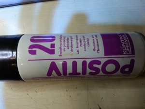
Positive-sprayed PCBs are regular PCBs that are covered by YOU with a thin layer of photo-sensitive laquer, using a POSITIV 20 spray, made by KONTAKT CHEMIE, in Germany.
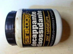
b. Decapant solution for soldering copper tubes. The best I have found is the italian “Saratoga decappante-disossidante” solution, but many other similar may be used;
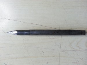
c. A 30W soldering iron, preferably with a ceramic tip;
d. NaOH, 7% solution, for developing the exposed PCBs;
e. FeCl3, in 30-40% solution, for etching the developed PCBs;
f. metallic thorn (best a tolls special steel);
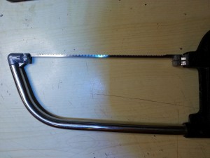
g. thin saw;
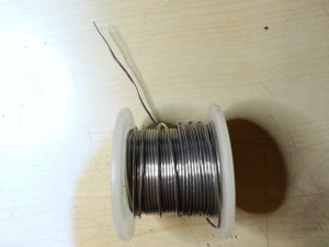
h. cored solder flux
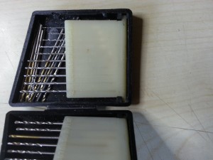
i. Drills. From 0.3mm to 2mm for through-holes;
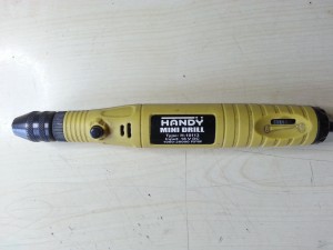
j. Small drilling machine with a mandrel that can hold drills from 0.3 mm to ~6 mm
k. UV light source.
2. STEPS TO OBTAIN THE PERFECT PCB
In the following I will demonstrate with a presensitive PCB all the steps described below.
a. CAD ELECTRONIC DRAWING
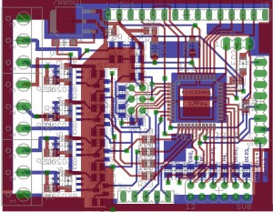
The CAD electronic drawing is obtained using Eagle, which can be utilized for free for small DIY projects.
Eagle is quite easy to learn and operate. Automatic cabling is a mess, but one can manually route all wiring to obtain very professional drawings to use for PCB manufacturing.
Eagle PCB Drawing.
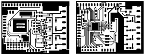
Top and Bottom sides in Black and White
b. PCB DRAWING PRINTOUT
I have used all kind of printers in order to achieve the best results. My experience says that inkjet printers, made by EPSON or SEIKO are among the best. The worst ones are HP printers, because they do not allow for precise customization of the printout.
Prints should be:
– printed on ink-jet transparencies. The rugged surface of the transparency should be the one printed.
– the paper should be selected as “EPSON MATTE” or “PHOTO PAPER MATTE”;
– the quality should be “BEST”;
– the speed should be “LOW”; Always disable high-speed printing;
– the print should be made in black only (or gray-scale);
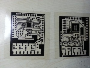
Printouts.
After printing, cut the drawing with scissors, leaving ~1cm (1/2 inch) on each margin.
After this operation, please shut off the lights in your laboratory, close the blinds if there is strong sun outdoors. You may leave a small light source for environmental lightning, just enough to see what you are doing and nothing else.
b. PCB PREPARATION
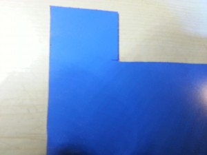
There is no need to make special preparations for Presensitive PCBs, as the only thing to do is to remove the blue protective layer just before exposing the PCB.
PCB sprayed with POSITIV 20 should be left to dry for AT LEAST ONE FULL DAY (24 hours). Even if the instructions on POSITIV20 say you can use the PCB right away, in practice I have found this not to be true at all.
Just saw your PCB to be 2-3 mm larger on each side than your drawing.
Put your PCB on a long ruler ( I use a 40cm one) and gently put the transparency drawing over the PCB, aligning the drawing with the PCB. Your drawing should be in the middle of the PCB.
For double-layered PCBs, you should always start with just one side of the PCB. The second side will be dealt with later in this documentations.
c) Preset the timer on your Ultraviolet (UV) light source.
The exposing times are as follows:
– for 100W UV bulbs:
– 2 minutes for presensitive PCBs;
– 30 seconds for POSITIV20 sprayed PCBs;
– for UV leds:
– 6 minutes for presensitive PCBs;
– 1 minute 30 seconds for POSITIV20 sprayed PCBs;
Remember, if you use an UV bulb (bulb with mercury discharge and a buck driver), it should be left running for at least 3 minutes before exposing the PCB. UV Led exposure do not need this time.
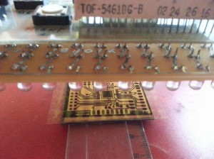
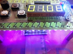
Print under the UV exposure device.
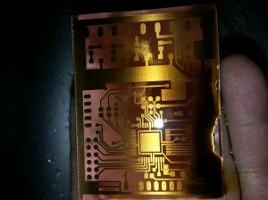
Print being exposed to UV light.
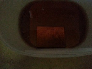
Use an ice cream plastic box, filled with enough NaOH solution 7% to cover the PCB.
Put your recently exposed PCB in the box and start shaking until you see the unexposed parts dissolving, leaving the useful wiring visible.
This operation can take 1-4 minutes. Wash thoroughly with a sponge soaked in soap and then rinse with water. You should have a small amount of FeCl3 in a cap. From time to time, pour several drops of FeCl3 on the PCB and see if it starts to etch the PCB. If the PCB is soaked with water, the FeCl3 will expand on the whole surface, leaving marks on the copper that was just developed.
You may also use a head lens to see if there are undeveloped areas on the PCB. Instead of re-immersing the PCB in NaOH, you should use that sponge and wash the PCB again, insisting on the areas that are not attacked by FeCl3, rinsing them, reapplying FeCl3 to see the effect. In rare cases the PCB needs supplementary immersion in NaOH if the development process was insufficient.
The final check is done using a lens.
d) Once the surfaced to be etched were attacked by FeCl3, just discard the NaOH solution (or keep it for future PCBs), rinse the ice-cream box, fill it with FeCl3 to about 2cm (~1 inch) .
Use paper towels to dry the recently developed PCB.
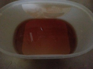
Put it on the surface of the FeCl3 solution, with the side to be etched downwards, and leave it float on the surface of the FeCl3 solution. Indeed, surface forces will keep the PCB afloat and will not let it drown, if the PCB was previously dried well enough.
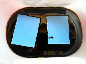
Etching the top side of the PCB. The PCB is floating on the surface of the liquid, allowing the copper chloride to sink and generating a natural movement of the solution.
On single-sided PCBs, one can see how the copper disappears, by checking the PCB, after 10-40 minutes, depending on the concentration of the FeCl3 solution, temperature and width of the copper clad.
On double sided PCBs, one can not see the first layer being etched. The PCB should be first checked after 20 minutes, and every 5 minutes afterwards, until the etching of the first side is complete.
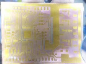
Top side etched
e1) JUST FOR DOUBLE LAYERED PCBs
– use the metallic thorn to mark some holes on all four sides of the PCB;
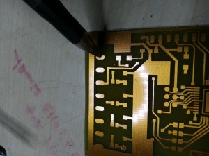
Marking holes with a metallic thorn
– drill those holes using the right drills; Best to drill large and thin holes too. USE YOUR BEST CUT DRILL BITS. LEAVE THE HOLES AS THEY ARE. YOU MAY DAMAGE THE PRESENSITIVE LACQUER. If the shoulders of the holes are too high, cut them using a drill a little bit larger that the one used to drill the holes, BY HAND.
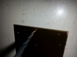
Holes drilled in the corners of the PCB
Hole shoulder removal using a larger drill, by hand
– develop the second side of the PCB according to the same instructions above;
– REDRAW THE SIDES OF THE HOLES on the second side of the PCB with a permanent marker of the right width and using head lenses, if needed.
Bottom side check after UV exposure and developing
– etch the second side of the PCB according to the same instructions above;
Bottom side etched and cleaned with isopropyl alcohol
e2) JUST FOR ALUMINUM-BASED PCBs.
The ferric chloride reacts heavily with aluminum. Thus, all aluminum surfaces MUST be protected before the etching process. I use duct tape for this, which is very adhesive and doesn’t let the solution to gain the aluminum substrate. Be very careful at the edges of the PCB, where the solution has a stronger tendency to infiltrate.
Also, aluminum-based PCBs cannot be etched afloat. Because of the higher density of the aluminum, the PCB will naturally sink in the solution. These PCBs should be immersed vertically in the solution, using a narrow recipient. The PCB should also be turned upside down every 5 minutes, because the copper chloride that develops during the etching process has a tendency to glue to the lower part of the PCB and the etching process becomes harder in this area.
Aluminum-based PCBs DO NOT SUPPORT THROUGH HOLES. A through hole will connect electrically the aluminum base and the copper clad, rendering the whole PCB unusable. Aluminium-based PCBs should be used only with copper islands for remote connection, all components should be surface mounted, with no hole drilled.
f) clean thoroughly the PCB with isopropyl alcohol. Cetones could also be used (nail polish remover=acetone) but they are very flammable, they vaporize very quickly and are highly flammable.
g) after having marked all the holes and then drilled them all, use a cutter to even the holes edges.
h) put soldering paste all over your PCB (one side at a time);
i) use the soldering iron with minute quantities of tin to cover all the tracks on the PCB.
Most people skip this phase, but IMHO it is one of the most important because:
– this will allow later for a better soldering and it will not allow the copper layer(s) to oxidize;
– if one covers the tracks one by one, it is easy to observe shorts or very fine interruptions;
– decapant paste contains also some wax, which will not allow later for the tin to spread from one pin to another so easily;
– in the long run, it prevents copper oxide to appear, because of the humidity in the air combined with different salts;
– it allows for better and faster soldering when planting the parts.
– it obliges a through inspection of every track, allows for quick repairs and avoids taking out parts for later repairs.
Decapant paste on PCB
Tinning the copper tracks
j) wash thoroughly the soldering paste. THOROUGHLY! WITH SOAP AND SPONGE! Soldering paste conducts electricity and you don’t want any bizarre electrical behavior.
Tinned PCB. Final result on one side
k) mark the holes using the metallic thorn;
l) drill the holes;
Holes drilled with different sizes of drills. Through-holes are drilled with a 0.4 mm drill
m) plant the electronic parts:
– through-holes if double sided;
Through-hole wire soldering
– straps if single sided;
– passive components;
Passive components soldering
– voltage regulators, verify voltages;
– active components (transistors, diodes, ICs).
That’s it! Good luck making PCBs!
