Jun 302014
 

Timer for Ultraviolet exposure with UV LEDs and PWM fine tuning

Timer operation video

Timer measurement video

Previous timer projects had only on/off possibilities for the UV leds. Some projects need a finer tuning of the UV value, and I am not talking just about PCBs. Stamps and other things need ultraviolet curing, with setups that cannot be fulfilled using the basic, previous design.

Based on the same hardware as the Common Cathode timer available in this post, I have further developed the software in order to use the same hardware to achieve finer results.

This is how it works:

 1. Countdown timer setup mode

When powered, the display shows in minutes and seconds a predefined value of 5:00 (five minutes, zero seconds). The display is blinking and the second dot point is lit, showing that it is in countdown timer setup mode.

This value may be modified using the left and right keys (to decrease or to increase the timer). The steps are measured in seconds. The maximum value that can be programmed is 99 minutes and 59 seconds, just as much as the display can hold with just 4 digits.

The UV leds and the blue witness led are shut off.

Pressing the GO key will enter in countdown timer mode.

2. PWM setup mode

GO and RIGHT keys pressed simultaneously switch the countdown value to the PWM value, expressed in percents (from 0% to 100%).

The default value is 100 (%).

The display is blinking and the fourth dot point is lit, showing that it is in PWM value setup mode.

This value may be modified using the left and right keys (to decrease or to increase the PWM value). The steps are measured in percents. The maximum value that can be programmed is 100%.

The UV leds and the blue witness led are lit at the value defined by the PWM value.

To switch back to displaying the countdown timer, press GO and LEFT keys simultaneously.

Pressing the GO key will enter in countdown timer mode.

3. Countdown Timer mode

Pressing the GO key while in either setup mode (countdown timer, PWM) or in power save mode will enter in countdown timer mode.

The display is steady (does not blink), the second dot point is lit and it shows the minutes and seconds as they go down to zero. The display is reverted to minutes and seconds, no matter which was the mode when the GO key was pressed.

The UV leds and the witness blue led are lit at the defined PWM value;

At the end of the countdown, the UV lights are shut off, the device enters timer countdown setup mode and emits 10 beeps to let the user know it has terminated its timing job.

During Countdown timer mode, the power save mode is disabled and keys functions are also disabled. Upon reaching zero, keys functions are enabled again and power save mode enters automatically in effect after ~ 10 seconds.

4. Power save mode

To save power and to allow the 78L05 regulator to cool down after counting down, the display is shut off after 10 seconds and just the dot point remains blinking. Power save mode works no matter if you are in timer setup mode or in PWM setup mode.

5. Memorizing other values as default values

LEFT and RIGHT keys pressed simultaneously will write in EEPROM both the timer countdown value and the PWM value. set up by the user. At the next power-up, these will be the values used by default for countdown and PWM. After writing these values in EEPROM, the device emits 4 beeps.

6. Other considerations
I can assure you the 78L05 will function very well over time. However, if you feel any doubt, replace it with an 7805 and a small aluminum heat sink.

Any key will do exactly as intended and, if pressed, will disable the power down mode.

During power down, a beep is emitted every ~10 seconds to let the user know the device is waiting, asleep.

The code is written in C and compiles under AVR Studio 4.

The fuses for ATtiny2313 are set as follows:

SELFPREGEN - disabled
DWEN       - disabled
EESAVE     - disabled
SPIEN      - enabled
WDTON      - disabled
BODLEVEL   - brown-out detection disabled
RSTDISBL   - disabled
CKDIV8     - disabled
CKOUT      - disabled
SUT_CKSEL  - Internal RC Oscillator 8MHz; Start-up time: 14CK + 65 ms


Common Cathode Display Version: HEX and EEP compiled files enabling you to have a full featured timer, can be found here.

Common Anode Display Version: HEX and EEP compiled files enabling you to have a full featured timer, can be found here.


The complete source code for either CC version or CA version can be emailed to those interested in obtaining it. The cost is 10 EUR, payable by paypal, to Cristian Copcea, email copcea at yahoo dot com

Both (CC and CA versions) will be emailed for 15 EUR.

These funds will contribute to acquiring parts, equipment and all other necessary stuff (TIME being the most expensive) to create more interesting devices to be posted in this blog.


Make the transaction specifying “UV Timer with PWM source code”, send me an email about this and you will receive in return shortly an email from me with the desired source code(s) attached to the email in a .rar archive.


Jun 232014


PCB exposure with UV Leds and digital countdown timer DIY


I have worked for years with a mercury-discharge bulb for exposing PCBs and it started lately to show symptoms of old age.

I have decided to retire the old stuff and to replace it with a modern installation, using UV Leds and a digital timer.


A. PCB exposure with Ultraviolet LEDs

The idea is to make a LED matrix, powered at 12V from a regular adaptor.

The matrix should be big enough but not so big as to not having where to range it.

Finally I came up with a matrix of 110×80 mm (4.3×3.2 in), which is enough for most DIY projects.

UV array schematic

The leds, grouped by four, can be powered with 12V directly, since the forwarding voltage of a UV led is 3.3-3.6V.

Actually, at 12V, they are a little bit underpowered, but I see this as a benefit. Even if exposure time is increased a little bit, a digital timer can do the trick and make a sound when the whole process is finished, leaving me to other tasks. For POSITIV 20 PCBs, the initial exposure time was quite strict, which annoyed me because at every error I had to clean the PCB, spray it, leave it to cure for 24 hours – basically every error ate one full day. Prolonging the exposure time to 1:30-2:00 minutes means more finesse and less time and materials and nerves lost.

UV array PCB

The leds should be emitting somewhere around 380-400 nm and they can easily found very cheap on ebay. This array contains 168 UV leds.

B. Timer for the PCB exposure with Ultraviolet LEDs, with a Common Anode, 7 segments display

1. Schematic and PCB

The timer has at its heart an Atmel ATtiny2313 micro-controller that was hanging in a box, along with older and unused AT90S1200 and AT90S2313. These were disturbing me every time I looked into that box. Suddenly, I saw this small project as a challenge to try to return back to the community a few of the things I have learned, by making a small but easy-readable project which would also serve my purpose of retiring the old bulb.

ATtiny1200 was too small for the project, and AT90S2313 lacked one output at first glance.

I have decided then to use the ATtiny2313 to make a small yet effective schematic, compared to those found googling. It seems that little guy did its job well in the end.

The schematic:

Power. Classical schematic with a 78L05, 5V linear regulator

Micro-controller schematic

In the schematic, I have used AT90S2313, which is pin to pin compatible with ATtiny2313, excepting the XTAL lines. ATtiny2313 has a supplementary port, “A”, with three pins, with alternative functions on the XTAL and RESET pins. Two of the port A bits go to the XTAL pins if these are not used to drive a quartz and the third bit goes to the reset pin, if needed.

The buzzer has a 100 ohms resistor in series in order to limit the current drawn from the MCU pin, and a second, 1K, resistor, in parallel, in order to decrease the capacitive load of the buzzer (which is in fact a capacitor which sides are moving while powered). A led (red) shows that there is power. Another 10k resistor is tied to the RESET pin in order to keep it high while operating.

ISP header and keyboard schematic

The ISP header is tied to the MCU classically. The keyboard has just 3 keys, uses the same pins as the ISP and ties these pins to high level through 3 resistors, value 4.7 Kohms. I am using external resistors instead of the internal pull-ups because the internal pull-up resistors have, in my opinion, a too high resistance: 20-50 kohms for I/O pins and 30-60 kohms for the RESET pin.

The power driver for the UV leds

The UV leds are driven by a p-channel mosfet, which is driven by an npn transistor which is driven by the MCU itself. The npn transistor is necessary to shift the 0-5V from the MCU output to an 8-12V output, necessary to drive the gate of the mosfet. I use p-channel mosfets usually because they allow me to keep a common ground between the driver and the load, as opposed to n-channel mosfets. A blue led is the witness on the PCB, to know the UV leds are lit. It is wired in parallel with the whole UV led matrix and it is powered by the mosfet itself.

The p-channel mosfet is enough to drive a steady load of 4.5A at 30V. This is enough for driving directly a load composed of 200 leds powered at 12V, and even more if using PWM.

Common Anode Display Schematic

The display is a common anode one, found in another box, not multiplexed. I have tied all the segment outputs together to make it multiplexed. The display is tied directly to the MCU without using any transistors. Common anodes have 10 ohms resistors in series, to lower the current that passes through the display, without dimming it too much. A regular ATtiny2313 can withstand easily the current going through the display and just gets a little bit warmer while operating.

Actually, there is an error in the footprint of the display: the segments f and g are swapped, it was my error in the footprint design in Eagle. This mistake was solved in software, swapping f and g segments one more time.

If you wish to see the dot point (DP) blinking, to easier differentiate minutes from seconds, just wire the second DP pin to the ground. In the schematic and on the PCB this pin is in the air.

UV Timer PCB

The PCB is one-sided and contains just 8 straps and 1 wire wrapping for the Dot Point.

2. How it works – software

What can be learned from this small project:
- How to program several bits of a port as outputs and the others as inputs;
- How to use multi-dimensional data structures;
- How to program an Atmel MCU timer along with the prescaler in order to have
  well-timed repetitive events;
- How to use an Atmel MCU interrupt routine;
- How to implement a power saving system to preserve our planet from useless
  energy consumption and also to cool down electronic parts by diminishing
  the load while in stand-by;
- How to set a particular bit in a port and how to clear a particular bit in
  a port;
- How to make software timers;
- How to use bit value macros;
- How to read keys and avoid over-reads by using small delays;
- How to reuse pins in an MCU project;
- How to use functions in order to have very small, but intelligible main
  routines;
- How to read and write from/to EEPROM;
- how to alter default values for direct usage upon power-up.

Just read the code, it is in my opinion very readable and self-explainable,
even for a newbie.


Operation:

When powered, the display shows in minutes and seconds a predefined value of 5:00. The display is blinking, showing that it is ready to be either programmed, or to start counting.

This value may be modified using the left and right keys (to decrease or to increase the timer). The steps are measured in seconds. The maximum value that can be programmed is 99 minutes and 59 seconds, just as much as the display can hold with just 4 digits.

To memorize in EEPROM the actual value, press LEFT and RIGHT keys simultaneously. At the next power-up, this will be the value used by default for countdown.

When pressing the “GO” key, the system:

– lits the UV leds and the witness blue led;

– starts counting downwards, to 0:00

– the display is not blinking anymore, nor is it shut

At the end of the countdown, the UV lights are shut, the display is blinking again and emits 10 beeps to let the user know it has terminated its job.


To save power and to allow the 78L05 regulator to cool down, the display is shut off after 10 seconds and just the dot point remains blinking.

I can assure you the 78L05 will function very well over time. However, if you feel any doubt, replace it with a 7805 and a small aluminum heat sink.

Any key will do exactly as intended and, if pressed, will disable the power down phase.

During power down, a beep is emitted every ~10 seconds to let the user know the device is waiting, asleep.

The code is written in C and compiles under AVR Studio 4.

The fuses for ATtiny2313 are set as follows:

SELFPREGEN - disabled
DWEN       - disabled
EESAVE     - disabled
SPIEN      - enabled
WDTON      - disabled
BODLEVEL   - brown-out detection disabled
RSTDISBL   - disabled
CKDIV8     - disabled
CKOUT      - disabled
SUT_CKSEL  - Internal RC Oscillator 8MHz; Start-up time: 14CK + 65 ms

The code:

#include <avr/io.h>
#include <avr/interrupt.h>
#include <avr/eeprom.h>
#define F_CPU 80000000
#include <util/delay.h>

#define SEG_a 0x01
#define SEG_b 0x02
#define SEG_c 0x04
#define SEG_d 0x08
#define SEG_e 0x10
#define SEG_f 0x20
#define SEG_g 0x40
#define SEG_dot 0x80

uint16_t EEMEM Edigit=800;
uint16_t Def_digit=300;

//global variables for isr()
uint16_t digit, decimal, digit_addressed=0;
uint8_t d[8];
uint8_t pulsing=0;
uint16_t pulseinterval;
uint16_t maxpulseinterval=512;
uint16_t ProgrammedDigit=0;
uint8_t LedOn=0;

//keys definition
#define GO        7
#define RIGHT     6
#define LEFT     5
#define KPIN  PINB
uint8_t keypressed=1;        //a key was pressed
uint8_t t1=0;
uint8_t Powersave=0;

//character definition
unsigned char seg[]=
{
    (SEG_a|SEG_b|SEG_c|SEG_d|SEG_e|SEG_g),             // 0
    (SEG_b|SEG_c),                                     // 1
    (SEG_a|SEG_b|SEG_d|SEG_e|SEG_f),                 // 2
    (SEG_a|SEG_b|SEG_c|SEG_d|SEG_f),                 // 3
    (SEG_b|SEG_c|SEG_c|SEG_f|SEG_g),                 // 4
    (SEG_a|SEG_c|SEG_d|SEG_f|SEG_g),                 // 5
    (SEG_a|SEG_c|SEG_d|SEG_e|SEG_f|SEG_g),             // 6
    (SEG_a|SEG_b|SEG_c),                             // 7
    (SEG_a|SEG_b|SEG_c|SEG_d|SEG_e|SEG_f|SEG_g),     // 8
    (SEG_a|SEG_b|SEG_c|SEG_d|SEG_f|SEG_g),             // 9
    (SEG_dot),                                             // NULL DISPLAY FOR POWER SAVE
};

//interrupt routine for character display
ISR(TIMER0_OVF_vect)
{
    pulseinterval++;
    if (pulseinterval>maxpulseinterval) pulseinterval=0;
    if ((pulsing==1) && (pulseinterval < maxpulseinterval/2))
    {
        PORTB=(0<<DDB0) | (0<<DDB1)| (0<<DDB2)| (0<<DDB3);
    }
    else
    {    
        PORTD = ~(d[digit_addressed]);
        switch (digit_addressed)
        {
            case 0: PORTB=(1<<DDB0) | (0<<DDB1)| (0<<DDB2)| (0<<DDB3);
            break;
            case 1: PORTB=(0<<DDB0) | (1<<DDB1)| (0<<DDB2)| (0<<DDB3);
            break;
            case 2: PORTB=(0<<DDB0) | (0<<DDB1)| (1<<DDB2)| (0<<DDB3);
            break;
            default:PORTB=(0<<DDB0) | (0<<DDB1)| (0<<DDB2)| (1<<DDB3);
        }
        if (LedOn==1) PORTB |= (1<<DDB4);
        digit_addressed++;
        if(digit_addressed>=4) digit_addressed=0;
    }
}

void display(void)
{
    uint8_t min, sec;
    if (Powersave!=1)
    {
        min=digit/60;
        sec=digit-min*60;

        //computing digits
        d[4]=min/10;
        d[5]=min-d[4]*10;
        d[6]=sec/10;
        d[7]=sec-d[6]*10;

        d[0]= seg[d[4]];
        d[1]= seg[d[5]];
        d[2]= seg[d[6]];
        d[3]= seg[d[7]];
    }
    else
    {
        d[0]= seg[10];
        d[1]= seg[10];
        d[2]= seg[10];
        d[3]= seg[10];
    }
}

void init(void)
{
    TCNT0 = 0x00 ;
    TCCR0B = 0x03; //prescaler of 64
    TIMSK = 0x02; //overflow irq req'd
    sei();

    DDRA =1;
    PORTA=7;

    PORTB|=_BV(0)|_BV(1)|_BV(2)|_BV(3)|_BV(4);
    DDRB |=_BV(0)|_BV(1)|_BV(2)|_BV(3);

    PORTD=0xff;
    DDRD =0xff;
    pulsing=1;                //pulsing
    pulseinterval=0;
    digit= eeprom_read_word(&Edigit);
    if (digit==0xFFFF)        //not programmed EEPROM
    {
        digit=Def_digit;
        eeprom_write_word(&Edigit, Def_digit);
    }

                    //set default value 
    display();                //starting value
    ProgrammedDigit=digit;    //if there is no delay programming, that one is the default value of 240s

}

void beep(void)
{
    PORTA=7;
    _delay_ms(10);
    PORTA=6;
    _delay_ms(30);

}

void readkeys(void)
{
    uint16_t i,j;
//LEFT AND RIGHT keys

//LEFT key
    if (bit_is_clear(KPIN, LEFT) && bit_is_clear(KPIN, RIGHT))
    {
        eeprom_write_word(&Edigit, digit);
    }
    else
    if bit_is_clear(KPIN, LEFT) 
    {
        keypressed=1;
        digit--;
        if (digit==0xFFFF) digit=0;
        ProgrammedDigit=digit;
    }
    else
//RIGHT key
    if bit_is_clear(KPIN, RIGHT) 
    {
        keypressed=1;
        digit++;
        if (digit>5999) digit=5999;
        ProgrammedDigit=digit;
    }
    else
        if bit_is_clear(KPIN, GO) 
    {
        keypressed=1;
        Powersave=0;
        PORTA=7;
        _delay_ms(10);
        PORTA=6;
        _delay_ms(30);
        LedOn=1;
        pulsing=0;
        ProgrammedDigit=digit;
        for (i=0;i<ProgrammedDigit;i++)
        {
            _delay_ms(104);
            digit--;
            display();
        }
        digit=ProgrammedDigit;
        display();
        pulsing=1;
        LedOn=0;
        for(j=0; j<10; j++)
        {
            beep();
        }
        pulsing=1;
    }
    else    keypressed=0;

}

void testfordisplaysleep(void)
{
    if (keypressed==0)    //if there is no key pressed
    {
        t1++;            
        if (t1==170)    //wait ~10 seconds
        {
            t1=0;        
            beep();        //beep every ~10 seconds while sleeping
            Powersave=1;//and put display to sleep
        }
    }
    else                //on any key press 
    {    
        t1=0;            
        Powersave=0;    //wake up display
    }
}

int main()

{
    init();
    _delay_ms(10);
    LedOn=0;
    PORTA=6;
    t1=0;
    keypressed=1;
    while(1)
    {
        readkeys();            //read key
        display();            //display number
        _delay_ms(6);        //wait a little bit
        testfordisplaysleep();
    }

}

The complete AVR4 project for the common anode display timer, without the EEPROM functionality, can be downloaded here.

In order to add this functionality to your project, copy and paste the code above over the UV_Timer.c file and recompile with AVR Studio 4.


3. The actual device

UV LED matrix

UV Leds and timer assembled

C. Timer for the PCB exposure with Ultraviolet LEDs, with a Common Cathode, 7 segments display

1. Schematic and PCB

The schematic is similar to the first version:

5V Power stage

ATtiny2313 connections

Here, one modification was made: the DP from the display was tied to the A1 pin.

Keyboard and ISP connectors

Mosfet Power Stage

Common Cathode Display

PCB

2. Software

Basically the software is the same as the common anode version, with the following differences:

a. The multiplex routine in ISR works with a negative logic, because of the common cathode. Digits definitions are also updated to the same negative logic. How does it work: we don’t lit anymore the segments to be lit, but we keep them off and lit all the other segments. Because of the polarity reversal on the display, our negative logic is inverted one more time. The result is that the segments defined to be off will in fact lit, leading to a positive image in the end.

b. Supplementary lines were added to solve the issue of the dot point. Since all dot points are wired together, the simpler solution used previously cannot be applied anymore. I have used the A1 bit of the ATtiny2313 to cope with the dot point. This bit must also be part of the multiplex routine, since we wish to lit only the second dot point and keep all other dot points off. Moreover, the A0 bit is used for activating the buzzer in all phases of the display: while on, blinking or in power save mode. This required the usage of specific bit processing while multiplexing. I’ll let you discover in the code the usage of specific bit processing, i.e. “setting the bit” and “clearing the bit”, while all the other bits remain unchanged.

The code:

#include <avr/io.h>
#include <avr/interrupt.h>
#include <avr/eeprom.h>
#define F_CPU 80000000
#include <util/delay.h>

#define SEG_a 0x01
#define SEG_b 0x02
#define SEG_c 0x04
#define SEG_d 0x08
#define SEG_e 0x10
#define SEG_f 0x20
#define SEG_g 0x40
#define SEG_dot 0x80

uint16_t EEMEM Edigit=800;
uint16_t Def_digit=300;

//global variables for isr()
uint16_t digit, decimal, digit_addressed=0;
uint8_t d[8];
uint8_t pulsing=0;
uint16_t pulseinterval;
uint16_t maxpulseinterval=512;
uint16_t ProgrammedDigit=0;
uint8_t LedOn=0;

//keys definition
#define GO        7
#define RIGHT     6
#define LEFT     5
#define KPIN  PINB
uint8_t keypressed=1;        //a key was pressed
uint8_t t1=0;
uint8_t Powersave=0;

//character definition
unsigned char seg[]=
{
    //negative logic
    (SEG_g),                                         // 0
    (SEG_a|SEG_d|SEG_e|SEG_f|SEG_g),                // 1
    (SEG_c|SEG_f),                                     // 2
    (SEG_e|SEG_f),                                     // 3
    (SEG_a|SEG_d|SEG_e),                             // 4
    (SEG_b|SEG_e),                                     // 5
    (SEG_b),                                         // 6
    (SEG_d|SEG_e|SEG_f|SEG_g),                        // 7
    (SEG_dot),                                         // 8
    (SEG_e),                                         // 9
    (SEG_a|SEG_b|SEG_c|SEG_d|SEG_e|SEG_f|SEG_g)     // NULL DISPLAY FOR POWER SAVE
};

//interrupt routine for character display
ISR(TIMER0_OVF_vect)
{
    pulseinterval++;
    if (pulseinterval>maxpulseinterval) pulseinterval=0;
    if ((pulsing==1) && (pulseinterval < maxpulseinterval/2))
    {
        PORTB=(1<<DDB0) | (1<<DDB1)| (1<<DDB2)| (1<<DDB3);
    }
    else
    {    
        PORTD = ~(d[digit_addressed]);

        switch (digit_addressed)
        {
            case 0: {PORTB=(0<<DDB0) | (1<<DDB1)| (1<<DDB2)| (1<<DDB3); PORTA=PORTA&~_BV(1);}     //clear bit 1 port a
            break;
            case 1: {PORTB=(1<<DDB0) | (0<<DDB1)| (1<<DDB2)| (1<<DDB3); PORTA|=_BV(1);}         //set   bit 1 port a
            break;
            case 2: {PORTB=(1<<DDB0) | (1<<DDB1)| (0<<DDB2)| (1<<DDB3); PORTA=PORTA&~_BV(1);}    //clear bit 1 port a
            break;
            default:{PORTB=(1<<DDB0) | (1<<DDB1)| (1<<DDB2)| (0<<DDB3); PORTA=PORTA&~_BV(1);}    //clear bit 1 port a
        }
        if (LedOn==1) PORTB |= (1<<DDB4);
        digit_addressed++;
        if(digit_addressed>=4) digit_addressed=0;
    }
}

void display(void)
{
    uint8_t min, sec;
    if (Powersave!=1)
    {
        min=digit/60;
        sec=digit-min*60;

        //computing digits
        d[4]=min/10;
        d[5]=min-d[4]*10;
        d[6]=sec/10;
        d[7]=sec-d[6]*10;

        d[0]= seg[d[4]];
        d[1]= seg[d[5]];
        d[2]= seg[d[6]];
        d[3]= seg[d[7]];
    }
    else
    {
        d[0]= seg[10];
        d[1]= seg[10];
        d[2]= seg[10];
        d[3]= seg[10];
    }
}

void init(void)
{
    TCNT0 = 0x00 ;
    TCCR0B = 0x03; //prescaler of 64
    TIMSK = 0x02; //overflow irq req'd
    sei();

    DDRA =3;
    PORTA=_BV(0)|_BV(1)|_BV(2);    //all 3 bits of PORT A are set -> DP lit, beep on
    PORTB|=_BV(0)|_BV(1)|_BV(2)|_BV(3)|_BV(4);
    DDRB |=_BV(0)|_BV(1)|_BV(2)|_BV(3);

    PORTD=0xff;
    DDRD =0xff;
    pulsing=1;                //pulsing
    pulseinterval=0;
    digit= eeprom_read_word(&Edigit);
    if (digit==0xFFFF)        //not programmed EEPROM
    {
        digit=Def_digit;
        eeprom_write_word(&Edigit, Def_digit);
    }

                    //set default value 
    display();                //starting value
    ProgrammedDigit=digit;    //if there is no delay programming, that one is the default value of 240s

}

void beep(void)
{
//    PORTA=7;
    PORTA|=_BV(0);            //enable beep
    _delay_ms(10);
//    PORTA=6;
    PORTA=PORTA& ~_BV(0);    //disable beep
    _delay_ms(30);

}

void readkeys(void)
{
    uint16_t i,j;
//LEFT AND RIGHT keys

//LEFT key
    if (bit_is_clear(KPIN, LEFT) && bit_is_clear(KPIN, RIGHT))
    {
        eeprom_write_word(&Edigit, digit);
    }
    else
    if bit_is_clear(KPIN, LEFT) 
    {
        keypressed=1;
        digit--;
        if (digit==0xFFFF) digit=0;
        ProgrammedDigit=digit;
    }
    else
//RIGHT key
    if bit_is_clear(KPIN, RIGHT) 
    {
        keypressed=1;
        digit++;
        if (digit>5999) digit=5999;
        ProgrammedDigit=digit;
    }
    else
        if bit_is_clear(KPIN, GO) 
    {
        keypressed=1;
        Powersave=0;
//        PORTA=7;
        PORTA=_BV(0)|_BV(1)|_BV(2);
        _delay_ms(10);
//        PORTA=6;
        PORTA=_BV(1)|_BV(2);
        _delay_ms(30);
        LedOn=1;
        pulsing=0;
        ProgrammedDigit=digit;
        for (i=0;i<ProgrammedDigit;i++)
        {
            _delay_ms(100);
            digit--;
            display();
        }
        digit=ProgrammedDigit;
        display();
        pulsing=1;
        LedOn=0;
        for(j=0; j<10; j++)
        {
            beep();
        }
        pulsing=1;
    }
    else    keypressed=0;

}

void testfordisplaysleep(void)
{
    if (keypressed==0)    //if there is no key pressed
    {
        t1++;            
        if (t1==170)    //wait ~10 seconds
        {
            t1=0;        
            beep();        //beep every ~10 seconds while sleeping
            Powersave=1;//and put display to sleep
        }
    }
    else                //on any key press 
    {    
        t1=0;            
        Powersave=0;    //wake up display
    }
}

int main()

{
    init();
    _delay_ms(10);
    LedOn=0;
    PORTA=_BV(1)|_BV(2);    //turn off beep, keep DP lit
    t1=0;
    keypressed=1;
    while(1)
    {
        readkeys();            //read key
        display();            //display number
        _delay_ms(6);        //wait a little bit
        testfordisplaysleep();
    }

}


The complete AVR4 project for the common cathode display timer can be downloaded here.

In order to add this functionality to your project, copy and paste the code above over the UV_Timer.c file and recompile with AVR Studio 4.

The Mosfet used in this project were both 9435 P-channel enhanced mode (30V/4A) Mosfets. The first version used a SOP-8 capsule while the second project used a TO-252 capsule. Since Eagle has parts with the same capsule and pin assignment for other parts, I have found uninteresting to make a library just for 9435. The datasheet for 9435 can be downloaded here.


3. The actual device

D. Timer for the PCB exposure with Ultraviolet LEDs, with a Common Cathode, 7 segments display and PWM

This is a further development of the the actual project in order to obtain a full-featured timer, and it is the subject of this post.


Jun 222014
 

State Of The Art Single Layer or Double Layer DIY PCB Production

with FR4 or aluminum substrate


After many years of DIY electronic projects, I can share my experience about having state of the art electronic PCBs, time after time, with zero or at least minimal initial errors.

I have chosen a double sided PCB as example, with a size of 50×37 mm (1.97×1.46 inches). This will show what to expect if following the instructions below.

If you like my tutorial, you know what to do.

The many things incurred in the process will be explained thoroughly and I wish you all the best results, similar to mine.


1. NECESSARY MATERIALS

a. presensitive PCBs or Positive-sprayed PCBs;

Presensitive PCBs are commercially available PCBs covered with a thin layer of photo-sensitive laquer, protected by a plastic layer which doesn’t allow for light to gain the photosensitive layer until the time of etching. These PCBs come in simple or double copper layered models.

Positive-sprayed PCBs are regular PCBs that are covered by YOU with a thin layer of photo-sensitive laquer, using a POSITIV 20 spray, made by KONTAKT CHEMIE, in Germany.

b. Decapant solution for soldering copper tubes. The best I have found is the italian “Saratoga decappante-disossidante” solution, but many other similar may be used;

c. A 30W soldering iron, preferably with a ceramic tip;

d. NaOH, 7% solution, for developing the exposed PCBs;

e. FeCl3, in 30-40% solution, for etching the developed PCBs;

f. metallic thorn (best a tolls special steel);

g. thin saw;

h. cored solder flux

i. Drills. From 0.3mm to 2mm for through-holes;

j. Small drilling machine with a mandrel that can hold drills from 0.3 mm to ~6 mm

k. UV light source.

l. Isopropyl alcohol

2. STEPS TO OBTAIN THE PERFECT PCB

In the following I will demonstrate with a presensitive PCB all the steps described below.

a. CAD ELECTRONIC DRAWING

The CAD electronic drawing is obtained using Eagle, which can be utilized for free for small DIY projects.

Eagle is quite easy to learn and operate. Automatic cabling is a mess, but one can manually route all wiring to obtain very professional drawings to use for PCB manufacturing.


Eagle PCB Drawing.

Top and Bottom sides in Black and White

b. PCB DRAWING PRINTOUT

I have used all kind of printers in order to achieve the best results. My experience says that inkjet printers, made by EPSON or SEIKO are among the best. The worst ones are HP printers, because they do not allow for precise customization of the printout.

Prints should be:

– printed on ink-jet transparencies. The rugged surface of the transparency should be the one printed.

– the paper should be selected as “EPSON MATTE” or “PHOTO PAPER MATTE”;

– the quality should be “BEST”;

– the speed should be “LOW”; Always disable high-speed printing;

– the print should be made in black only (or gray-scale);

Printouts.

After printing, cut the drawing with scissors, leaving ~1cm (1/2 inch) on each margin.

After this operation, please shut off the lights in your laboratory, close the blinds if there is strong sun outdoors. You may leave a small light source for environmental lightning, just enough to see what you are doing and nothing else.

b. PCB PREPARATION

There is no need to make special preparations for Presensitive PCBs, as the only thing to do is to remove the blue protective layer just before exposing the PCB.

PCB sprayed with POSITIV 20 should be left to dry for AT LEAST ONE FULL DAY (24 hours). Even if the instructions on POSITIV20 say you can use the PCB right away, in practice I have found this not to be true at all.

Just saw your PCB to be 2-3 mm larger on each side than your drawing.

Put your PCB on a long ruler ( I use a 40cm one) and gently put the transparency drawing over the PCB, aligning the drawing with the PCB. Your drawing should be in the middle of the PCB.

For double-layered PCBs, you should always start with just one side of the PCB. The second side will be dealt with later in this documentations.

c) Preset the timer on your Ultraviolet (UV) light source.

The exposing times are as follows:

– for 100W UV bulbs:

– 2 minutes for presensitive PCBs;

– 30 seconds for POSITIV20 sprayed PCBs;

– for UV leds:

– 6 minutes for presensitive PCBs;

– 1 minute 30 seconds for POSITIV20 sprayed PCBs;

Remember, if you use an UV bulb (bulb with mercury discharge and a buck driver), it should be left running for at least 3 minutes before exposing the PCB. UV Led exposure do not need this time.

Print under the UV exposure device.

Print being exposed to UV light.

Use an ice cream plastic box, filled with enough NaOH solution 7% to cover the PCB.

Put your recently exposed PCB in the box and start shaking until you see the unexposed parts dissolving, leaving the useful wiring visible.

This operation can take 1-4 minutes. Wash thoroughly with a sponge soaked in soap and then rinse with water. You should have a small amount of FeCl3 in a cap. From time to time, pour several drops of FeCl3 on the PCB and see if it starts to etch the PCB. If the PCB is soaked with water, the FeCl3 will expand on the whole surface, leaving marks on the copper that was just developed.

You may also use a head lens to see if there are undeveloped areas on the PCB. Instead of re-immersing the PCB in NaOH, you should use that sponge and wash the PCB again, insisting on the areas that are not attacked by FeCl3, rinsing them, reapplying FeCl3 to see the effect. In rare cases the PCB needs supplementary immersion in NaOH if the development process was insufficient.

The final check is done using a lens.

d) Once the surfaced to be etched were attacked by FeCl3, just discard the NaOH solution (or keep it for future PCBs), rinse the ice-cream box, fill it with FeCl3 to about 2cm (~1 inch) .

Use paper towels to dry the recently developed PCB.

Put it on the surface of the FeCl3 solution, with the side to be etched downwards, and leave it float on the surface of the FeCl3 solution. Indeed, surface forces will keep the PCB afloat and will not let it drown, if the PCB was previously dried well enough.

Etching the top side of the PCB. The PCB is floating on the surface of the liquid, allowing the copper chloride to sink and generating a natural movement of the solution.


On single-sided PCBs, one can see how the copper disappears, by checking the PCB, after 10-40 minutes, depending on the concentration of the FeCl3 solution, temperature and width of the copper clad.

On double sided PCBs, one can not see the first layer being etched. The PCB should be first checked after 20 minutes, and every 5 minutes afterwards, until the etching of the first side is complete.

Top side etched

e1) JUST FOR DOUBLE LAYERED PCBs

– use the metallic thorn to mark some holes on all four sides of the PCB;

Marking holes with a metallic thorn

– drill those holes using the right drills; Best to drill large and thin holes too. USE YOUR BEST CUT DRILL BITS. LEAVE THE HOLES AS THEY ARE. YOU MAY DAMAGE THE PRESENSITIVE LACQUER. If the shoulders of the holes are too high, cut them using a drill a little bit larger that the one used to drill the holes, BY HAND.

Holes drilled in the corners of the PCB

Hole shoulder removal using a larger drill, by hand

– develop the second side of the PCB according to the same instructions above;

– REDRAW THE SIDES OF THE HOLES on the second side of the PCB with a permanent marker of the right width and using head lenses, if needed.

Bottom side check after UV exposure and developing

– etch the second side of the PCB according to the same instructions above;

Bottom side etched and cleaned with isopropyl alcohol

e2) JUST FOR ALUMINUM-BASED PCBs.

The ferric chloride reacts heavily with aluminum. Thus, all aluminum surfaces MUST be protected before the etching process. I use duct tape for this, which is very adhesive and doesn’t let the solution to gain the aluminum substrate. Be very careful at the edges of the PCB, where the solution has a stronger tendency to infiltrate.

Also, aluminum-based PCBs cannot be etched afloat. Because of the higher density of the aluminum, the PCB will naturally sink in the solution. These PCBs should be immersed vertically in the solution, using a narrow recipient. The PCB should also be turned upside down every 5 minutes, because the copper chloride that develops during the etching process has a tendency to glue to the lower part of the PCB and the etching process becomes harder in this area.

Aluminum-based PCBs DO NOT SUPPORT THROUGH HOLES. A through hole will connect electrically the aluminum base and the copper clad, rendering the whole PCB unusable.  Aluminium-based PCBs should be used only with copper islands for remote connection, all components should be surface mounted, with no hole drilled.

f) clean thoroughly the PCB with isopropyl alcohol. Cetones could also be used (nail polish remover=acetone) but they are very flammable, they vaporize very quickly and are highly flammable.

g) after having marked all the holes and then drilled them all,  use a cutter to even the holes edges.

h) put soldering paste all over your PCB (one side at a time);

i) use the soldering iron with minute quantities of tin to cover all the tracks on the PCB.

Most people skip this phase, but IMHO it is one of the most important because:

– this will allow later for a better soldering and it will not allow the copper layer(s) to oxidize;

– if one covers the tracks one by one, it is easy to observe shorts or very fine interruptions;

– decapant paste contains also some wax, which will not allow later for the tin to spread from one pin to another so easily;

– in the long run, it prevents copper oxide to appear, because of the humidity in the air combined with different salts;

– it allows for better and faster soldering when planting the parts.

– it obliges a through inspection of every track, allows for quick repairs and avoids taking out parts for later repairs.

Decapant paste on PCB

Tinning the copper tracks

j) wash thoroughly the soldering paste. THOROUGHLY! WITH SOAP AND SPONGE! Soldering paste conducts electricity and you don’t want any bizarre  electrical behavior.

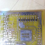
Tinned PCB. Final result on one side

k) mark the holes using the metallic thorn;

l) drill the holes;

Holes drilled with different sizes of drills. Through-holes are drilled with a 0.4 mm drill

m) plant the electronic parts:

– through-holes if double sided;

Through-hole wire soldering

– straps if single sided;

– passive components;

Passive components soldering

– voltage regulators, verify voltages;

– active components (transistors, diodes, ICs).


That’s it! Good luck making PCBs!


Switch to mobile version
Advertisment ad adsense adlogger